
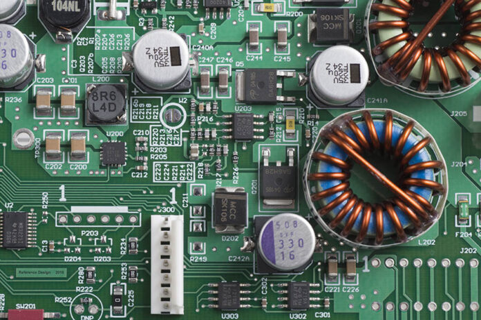
PCB design is a complex process that requires extreme precision and high levels of knowledge. Without a proper layout, you’re risking low performance and reduced functionality in all of your PCB projects.
If you’re an amateur looking to improve your PCB design, you’ve come to the right place! Here we’ll share important tips on how to keep your circuit boards functional, potent, and well-performing.
So, without any further ado, let’s get right to the bottom of it.
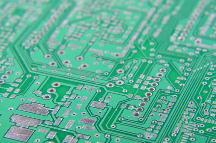
1. There should be sufficient space between traces
If you don’t want to experience short circuits during the assembly process, you’ll need to leave enough space between all of your components. This includes traces, holes, and adjacent pads, as you don’t want the wires to accidentally connect and create an electric shock, potentially frying your entire board.
Generally, the recommended space between all of your traces is anywhere between 0.006 to 0.010 inches. Anything out of this range is either too much or too little, in most cases.
2. 90-degree angles should be avoided entirely
Now, while some PCB designers and manufacturers still think this one’s debatable, we still think it’s better to be safe than sorry. Acute angles have been related to performance issues before, especially at high frequencies.
Overall, if you’d like to improve your PCB design, try avoiding 90-degree angles at all costs. There are many different ways you can “soften” those sharp edges, so do your research and try it out!
3. Switch to manual routing

Every advanced PCB design software has an automatic routine feature nowadays. However, depending on the complexity of your design, relying on these features is not always the best idea. Your experience and specific needs are more important than what the machine says. If you’re still going to use it, remember not to trust it blindly, and invest in a high-quality PCB designing program.
4. Choose a reliable manufacturer
The quality of your components may not directly fall into the designing process, but it’s nonetheless crucial to the entire project. Companies such as uetpcba.com can help you with both the designing and the manufacturing process with ease. If you’re working on a large-scale project, we recommend you seek help from professionals instead of trying to come up with a design yourself. It can save you from a lot of headaches later on.
Keep in mind that different manufacturers have different specs for their products, so make sure you’ve done your research before hiring any of them.
5. Use unique drill sizing symbols to simplify the entire process
Keeping everything organized is key to successful PCB designs. One of the ways you can achieve this is by using unique drill sizing symbols for different holes.
6. Choose a Turnkey PCB Assembly Company
Turnkey PCB assembly refers to a one-stop service for your project from design to procurement. FS Tech is a Chinese PCB company with turnkey services as its core. Buying services from them will give you the following advantages:
- Quality advantage: FS Tech has the same suppliers as the world’s top 500 companies
- Price advantage: The perfect supply chain system is that the price of FS Tech is lower than other companies
- Time advantage: From procurement to delivery, FS Techsaves a lot of time for your project
- Product diversity: FS Tech can make all types of boards, including flex boards, rigid boards, and flex-rigid boards
- Professional designer team: FS Tech not only has first-class after-sales service personnel, but also provides a professional designer for each customer.
Now, let’s say you have a couple of 0.023 diameter holes with different specifications (unique drill tolerance or plating requirements). It doesn’t matter they’re all 0.023, you’ll still need to use different symbols on the drawings if you want to make things easier later on.


")
